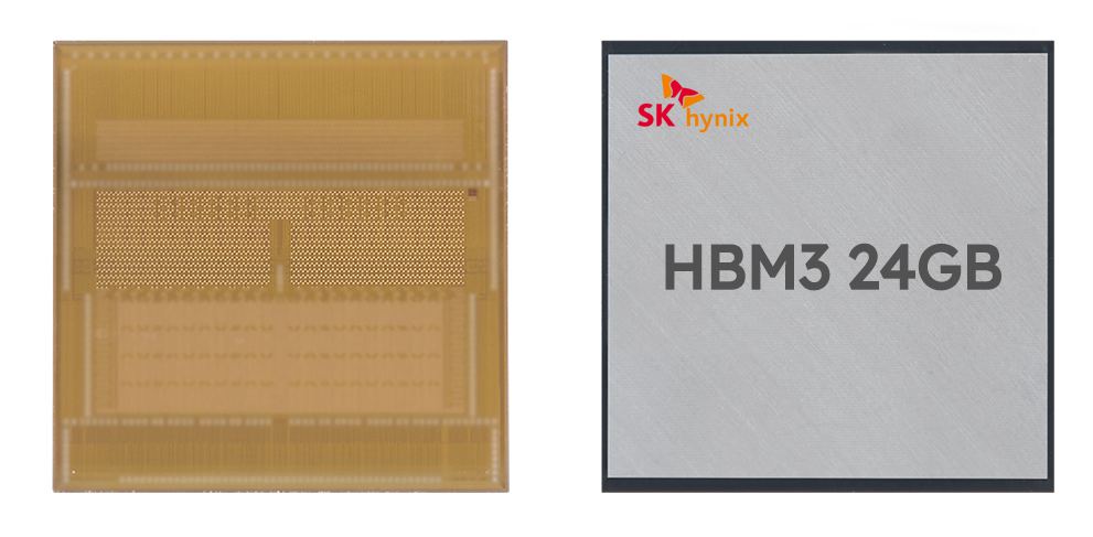
SK Hynix has developed the world's first 12 layer stacked HBM3 DRAM and has provided samples to customers
·Successfully developed the current highest capacity 24GB HBM3 DRAM product and is undergoing customer validation
·For the first time in the world, 12 single DRAM chips are vertically stacked, achieving high capacity and performance
·We will complete the mass production preparation within the first half of the year and "strengthen the leading position in the cutting-edge DRAM market"
April 20, 2023- SK Hynix (or 'company') announced on April 20 that it has once again surpassed the technical boundaries of the highest performance DRAM (memory) available - HBM3 *, achieving vertical stacking of 12 single DRAM chips for the first time in the world, successfully developing a new HBM3 DRAM product with a maximum capacity of 24GB (Gigabyte) * *, and is undergoing performance verification from customer companies.
*HBM (High Bandwidth Memory): A high value-added, high-performance product that vertically connects multiple DRAMs, significantly improving data processing speed compared to DRAM. The HBM DRAM products are developed in the order of HBM (first generation), HBM2 (second generation), HBM2E (third generation), and HBM3 (fourth generation).
**The maximum capacity of the existing HBM3 DRAM is 16GB vertically stacked with 8 single DRAM chips.
SK Hynix emphasized that "after the first global mass production of HBM3 DRAM in June last year, the company has successfully developed a 24GB package product with a capacity increase of 50%." Recently, with the development of the AI Chatbot industry, the demand for high-end storage has also increased. The company will launch it into the market from the second half of this year to meet market demand
The company's technical team has adopted advanced MR MUF * and TSV * * technologies for this new product. SK Hynix stated that advanced MR-MUF technology has strengthened process efficiency and product performance stability, and TSV technology has been used to vertically stack 12 single DRAM chips that are 40% thinner than existing chips, achieving the same height as 16GB products.
*MR-MUF: A packaging technology in which a liquid form of protective material is injected into the space of a semiconductor chip after stacking it to protect the circuit between the chip and the chip, and then solidified. Compared to the method of laying thin film materials on each stack of chips, the process efficiency is higher and the heat dissipation is more effective.
**TSV (Through Silicon Via) is an advanced packaging technology that punches thousands of fine holes into DRAM chips and connects the upper and lower chips through vertically connected electrodes. The SK Hynix HBM3 DRAM using this technology can transmit 163 Full HD movies per second, with a maximum speed of 819GB/s (819 gigabytes per second).
SK Hynix's HBM DRAM, which was first developed in the world in 2013, is a memory semiconductor product necessary for achieving generative AI that requires high-performance computing, and therefore has received high attention from the industry.
The latest specification of HBM3 DRAM has been evaluated as the preferred product for quickly processing large amounts of data, thus increasing the demand for large technology companies.
The company has provided 24GB HBM3 DRAM samples to several global customer companies for performance verification, and it is reported that customers have great expectations for this product.
Hong Xianghou, Vice President of SK Hynix Packaging and Testing (P&T), said, "Based on the world's top backend technology, the company has successively developed ultra high-speed and high-capacity HBM DRAM products. We will complete mass production preparations for new products in the first half of this year to consolidate our dominance in the cutting-edge DRAM market in the era of artificial intelligence
About SK Hynix
SK Hynix, headquartered in South Korea, is a leading global semiconductor supplier that provides semiconductor products such as DRAM (Dynamic Random Access Memory), NAND Flash (NAND Flash Memory), and CIS (CMOS Image Sensors) to customers worldwide. The company is listed on the Korean Stock Exchange, and its global depositary shares are listed on the Luxembourg Stock Exchange.