PCB assembly and welding technology
Key points of this article
·PCB assembly and welding can complete the physical circuit by selecting components, placing and welding components on the circuit board.
·In through-hole technology, electronic devices with pins or plug-in type are welded to the circuit board to form a circuit.
·Wave soldering is the most commonly used technology in THT and SMT PCBA

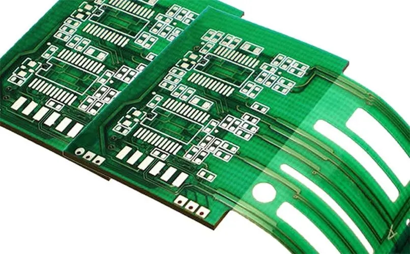
Printed circuit board (PCB) is an important part of electronic products; Without PCB, most electronic devices are just boxes that cannot be used. PCB is usually made of glass fiber and fixed together with epoxy resin. The PCB assembly and welding process completely constructs the physical circuit by selecting components, placing and welding components on the circuit board. Inspection, testing and feedback after PCB assembly and welding ensure that PCB can be successfully manufactured. In this article, we will discuss PCB assembly and soldering processes.
1. PCB assembly and welding
PCB assembly and welding process turns a circuit board into a functional prototype. PCB assembly stage includes device placement, welding, inspection, and finally testing. The PCBA process can be manual or automatic, depending on the manufacturer at each stage.
Brief description of PCBA process
PCB design starts from schematic diagram. PCB layout is designed according to the schematic diagram. PCB layout defines the electrical connection path (called routing) in the circuit and the placement position of components. Once the PCB layout design is approved, it will be printed.
The fabricated PCB is a glass fiber material sheet fixed together with epoxy resin. Wires made of copper are laid on the circuit board. The device is fixed on the circuit board through the welding process. The welding process uses a material called solder to hold the device in place. The PCB welded with the device constitutes an assembly PCB. After the device is attached to the PCB, it can be tested.
Three technologies are used in the PCBA process, which will be discussed one by one below.
2. PCB assembly technology
In the PCBA process, there are three key technologies:
Through hole technology (THT) PCBA process
In through-hole technology, electronic devices with pins or plug-in type are welded to the circuit board to form a circuit. The lead or terminal of the device is inserted through the hole or pad on the PCB and welded on the other side.
SMT PCBA process
There are two types of pads: through hole and surface mount. In PCBs that use surface mount pads, surface mount devices (SMDs) are soldered to form circuits. The welding surface is also the surface for placing devices with the aid of solder paste.
Mixed technology PCBA process
As circuit design becomes more complex, it is impossible to insist on using only one type of device in the circuit. In a PCB that implements complex circuits, there are both plug-ins and surface mount devices. This kind of PCB using hybrid devices is called hybrid technology circuit board, and its assembly process uses the hybrid technology PCBA process.
3. Through hole technology PCB assembly steps
The sequence of PCBA process varies according to the mounting technology used. Now let's discuss the steps of through hole PCB assembly.
01. Placement of components: In through-hole technology PCBA, engineers first place components in the corresponding positions given in PCB design documents.
02. Inspection and correction: After all components are placed, check the circuit board. During inspection, check whether the components are placed accurately. If it is found that the device is not placed accurately, such problems should be corrected immediately through correction steps. Inspection and correction must be completed before the welding process.
03. Welding: the next step in this process is welding, and the placed components are fixed on the corresponding bonding pad.
04. Test: After the PCB assembly and welding process is completed, the circuit board can be tested. Every PCB used in electronic equipment must go through this process and pass the test.
There are various welding technologies, and several of them will be discussed below.
4. Welding technology
No matter what mounting technology is used, all PCBA processes involve the welding process. A number of different types of welding techniques can be used to connect electrical components to PCBs, including:
Wave soldering: the most commonly used technology in THT and SMT PCBA
In wave soldering, PCB moves on a wave like liquid hot solder, and the solder will solidify and fix the device.
Brazing: the highest temperature and the strongest welding effect
In brazing, metal devices are attached by heating. However, this technology melts the metal at the bottom to accommodate the filler metal.
Reflow soldering
The reflow process uses heated solder paste to attach components to the circuit board. Solder paste in molten state connects pads and pins on PCB.
Soft soldering: a popular technology used to fix compact and fragile devices on printed circuit boards
In soft soldering, the metal space filler made of tin lead alloy is heated by an electric torch or gas to fix the device on the circuit board.
Hard welding: the welding effect is firmer than soft welding
Brazing is used to bond metal parts such as copper, brass, silver, or gold at a temperature of approximately 600 ° F.
During PCB assembly and welding, if there are design for manufacture (DFM) errors in PCB design, designers will have to go back to the layout process to solve these problems. This may happen many times, and many iterations will lead to severe design delay and waste of time, money and manpower. Good DFM design helps to maximize the smoothness of the entire design process, avoid accidents, and ensure the predictability of construction costs.


