Four key points of PCB wiring for surge protection
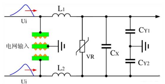
The position of the protective device is mainly set at the front end of the protected port. Especially when the port has multiple branches or loops, if the bypass or rear position is set, the protection effect and performance will be greatly reduced. In reality, we sometimes forget these problems because of insufficient location or for the aesthetic layout.
1、 Pay attention to the design surge current in PCB wiring
When testing, it is often encountered that the originally designed PCB cannot meet the surge requirements. General engineers only consider the functional design of the system when designing. For example, when the system actually works, it only needs to carry 1A current, and the design is based on this. However, it is possible that the system needs surge design, and the transient surge current should reach 3KA (1.2/50us&8/20us). Now, if I design according to the actual working current of 1A, can I achieve the above transient surge capacity? Practical and experienced projects tell us that this is impossible, so what can we do? The following calculation method can be used as a basis for PCB wiring to carry instantaneous current:
For example, for a 1oz copper foil with a width of 0.36mm, a 40us rectangular current surge occurs in a line with a thickness of 35um, and the maximum surge current is about 580A. If a 5KA (8/20us) protection design is required, the reasonable width of the front-end PCB wiring should be 2 oz copper foil 0.9mm. The width of the safety devices can be appropriately widened.
2、 Attention shall be paid to the safety spacing in the layout of surge port components
In addition to the safety distance designed according to the normal working voltage, we also need to consider the safety distance of transient surge.
We can refer to the relevant specifications of UL60950 for the safety distance during the design of normal operating voltage. In addition, we have specified in UL796 that the voltage withstand test standard of printed circuit board is 40V/mil or 1.6KV/mm. This data guide is very useful to set a safe distance between PCB wires that can withstand Hipot's withstand voltage test.
For example, according to Table 5B of 60950-1, the conductor between 500V operating voltages should meet the withstand voltage test of 1740Vrms, and the peak value of 1740Vrms should be 1740X1.414=2460V. According to the setting standard of 40V/mil, it can be calculated that the spacing between two PCB conductors should not be less than 2460/40=62mil or 1.6mm.
In addition to the normal precautions above, the surge should also pay attention to the size of the surge and the characteristics of the protective devices to increase the safety distance. The maximum cut-off creepage voltage is 2460V based on the 1.6mm distance. If our surge voltage is up to 6KV, or even 12KV, then whether the safety distance is increased depends on the characteristics of the surge overvoltage protective devices, This is also the loud noise that our engineers often make when they encounter surge creepage in experiments.
Taking ceramic discharge tube as an example, when 1740V withstand voltage is required, the device we choose should be 2200V, and its discharge peak voltage under the above surge condition is up to 4500V. At this time, according to the above calculation method, our safety distance is 4500/1600 * 1mm=2.8125mm
3、 Pay attention to the position of overvoltage protection devices in PCB
The position of the protective device is mainly set at the front end of the protected port. Especially when the port has multiple branches or loops, if the bypass or rear position is set, the protection effect and performance will be greatly reduced. In reality, we sometimes forget these problems because of insufficient location or for the aesthetic layout.

4、 Pay attention to the return path of high current
The large current return path must be close to the power supply ground or the earth of the housing. The longer the path is, the greater the return impedance is, and the greater the amplitude of ground level rise caused by the transient current. This voltage has a great impact on many chips, and is also the real culprit for system reset and locking.


